




What is the EL test for solar panels?
 Jul 01, 2025|
 View:1986
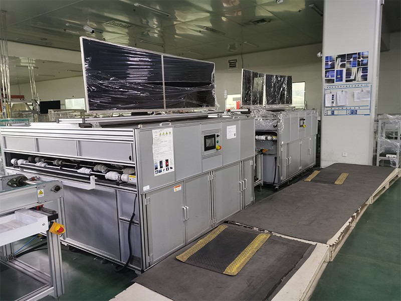
Electroluminescence (EL) testing has become an essential quality control and diagnostic tool in the photovoltaic industry. This non-destructive imaging technique allows manufacturers, installers, and maintenance professionals to detect various types of defects in solar panels that might otherwise remain invisible to the naked eye. By applying a forward bias voltage to solar cells in darkness and capturing the resulting infrared light emission, EL testing reveals the internal working condition of photovoltaic modules with remarkable clarity.
The Science Behind EL Testing
The fundamental principle behind EL testing lies in the photovoltaic effect working in reverse. When electrical current passes through a solar cell in the forward direction (opposite to normal operation), the cell emits infrared light through a process called electroluminescence. The intensity of this emission directly correlates with the local voltage across the cell, which in turn depends on the cell's material quality and electrical properties.
Areas with strong luminescence indicate properly functioning cell regions, while dark spots or irregular patterns reveal defects or performance issues. The wavelength of emitted light typically ranges between 950-1200 nm, requiring specialized infrared cameras for detection. This phenomenon occurs because the electrical current causes electrons and holes to recombine radiatively in the semiconductor material, releasing photons in the process.
Types of Defects Detectable by EL Testing
EL imaging can identify numerous solar panel defects that significantly impact performance and longevity:
Microcracks: Hairline fractures in silicon wafers that may not be visible to the naked eye but can severely impair electrical performance by interrupting current flow.
Broken cells: Complete fractures that separate cell portions, creating inactive areas that reduce power output.
Shunt defects: Localized areas of high leakage current that appear as dark spots in EL images due to reduced luminescence.
Material impurities: Inhomogeneities in the silicon wafer that affect charge carrier recombination and appear as dark regions.
Contact finger interruptions: Breaks in the metallic grid lines that collect current from the cell surface.
Potential induced degradation (PID): Characteristic darkening patterns that indicate performance degradation due to voltage stress.
Soldering defects: Poor interconnections between cells that create high-resistance areas.
Wafer defects: Crystal structure imperfections from the manufacturing process.

EL Testing Equipment and Setup
Conforming EL testing requires specific equipment and environmental conditions:
Power supply: A DC power source capable of providing current up to the panel's short-circuit current (Isc) rating, typically at 10-50% of Isc for optimal imaging.
Infrared camera: A high-resolution CCD or CMOS camera sensitive to near-infrared wavelengths, often cooled to reduce noise.
Dark environment: Testing must occur in complete darkness or with an enclosure to block ambient light.
Mounting system: Stable support for both the camera and panel, with adjustable positioning for optimal imaging.
Computer system: For image capture, processing, and analysis with specialized software.
Field-deployable EL systems have become increasingly compact, with some solutions incorporating all components into portable units for on-site inspections.
EL Testing Procedures
The standard EL testing protocol involves several key steps:
Panel preparation: Clean the panel surface and ensure electrical contacts are accessible.
Dark environment setup: Either perform testing at night or use a light-tight enclosure.
Electrical connection: Connect the power supply to the panel's output terminals, observing correct polarity.
Current application: Apply approximately 10-50% of the panel's rated short-circuit current.
Image capture: Position the IR camera perpendicular to the panel surface and capture high-resolution images.
Image analysis: Evaluate the EL images for uniformity and defect patterns using specialized software or expert interpretation.
Documentation: Record findings with reference images for quality records or maintenance reports.
Advantages of EL Testing
EL imaging offers numerous benefits for solar panel evaluation:
High sensitivity: Capable of detecting sub-millimeter defects that other methods might miss.
Non-destructive: Does not affect panel performance or void warranties.
Comprehensive: Provides a complete picture of all cells in a module simultaneously.
Quantitative: Allows for comparative analysis of defect severity and progression over time.
Versatile: Applicable throughout the panel lifecycle from manufacturing to field deployment.
Cost-effective: Identifies issues early, preventing more expensive failures later.

Limitations and Challenges
While powerful, EL testing has some limitations:
Darkness requirement: Needs complete darkness, which can be challenging for large-scale or daytime testing.
Current requirement: Panels must be accessible for electrical connection and able to handle the test current.
Surface temperature effects: Luminescence intensity varies with temperature, requiring consideration during analysis.
Interpretation complexity: Some defects require expert analysis to distinguish from normal variations.
Equipment cost: High-quality EL imaging systems represent a significant investment.
Limited depth information: Provides two-dimensional images without depth profiling of defects.
Applications in the Solar Industry
EL testing serves critical functions across the photovoltaic value chain:
Manufacturing quality control: Identifies production defects before panels leave the factory.
Incoming inspection: Verifies panel quality upon receipt at project sites or distribution centers.
Installation verification: Confirms panels weren't damaged during transport or installation.
Performance troubleshooting: Diagnoses underperforming systems in the field.
Warranty claims: Provides objective evidence for manufacturing or shipping damage claims.
Research and development: Evaluates new cell technologies and manufacturing processes.
Preventive maintenance: Detects developing issues before they cause significant performance loss.
EL Image Interpretation
Proper analysis of EL images requires understanding common patterns and their significance:
Uniform brightness: Indicates a healthy cell with consistent material properties.
Dark areas: Represent locations with reduced current flow or increased recombination.
Dark lines: Typically indicate cracks or breaks in the cell structure.
Bright edges: May show increased current density at cell peripheries.
Spotty patterns: Could indicate localized material defects or contamination.
Module-level patterns: Certain defects appear consistently across multiple cells, suggesting systemic issues.
Advanced analysis software can quantify defect areas, calculate performance impact estimates, and compare images over time for degradation monitoring.
Comparison with Other Testing Methods
EL testing complements other photovoltaic evaluation techniques:
Infrared thermography: While IR imaging detects temperature variations, EL shows electrical activity directly.
I-V curve tracing: Provides electrical performance data but without spatial defect information.
Visual inspection: Limited to surface defects visible to the naked eye.
UV fluorescence: Reveals specific material properties but different information than EL.
Photoluminescence: Similar principles but uses light excitation instead of electrical current.
EL testing often provides the most detailed information about cell-level defects affecting performance.
Future Developments in EL Testing
Emerging advancements in EL technology include:
Automated defect recognition: Machine learning algorithms for faster, more consistent image analysis.
Drone-based systems: Aerial EL imaging for large-scale solar farms.
Higher resolution cameras: Improved detection of microscopic defects.
Integrated testing solutions: Combining EL with other diagnostic methods in single platforms.
Real-time analysis: Faster processing for production line applications.
Standardized protocols: Industry-wide procedures for consistent results.
These developments promise to make EL testing more accessible and valuable throughout the solar industry.
Electroluminescence testing has become an indispensable tool for ensuring solar panel quality and performance. By revealing hidden defects and material inconsistencies, EL imaging helps maintain high system efficiency and longevity. As solar energy continues to grow globally, the role of EL testing in quality assurance and maintenance will only become more critical. With ongoing technological advancements making EL systems more capable and accessible, this diagnostic method will likely remain a cornerstone of photovoltaic evaluation for years to come.